10.5 Native Vt NMOS (Optional)
This section describes Native NMOS rules. This process supports 3.3V and 5V/6V native Vt NMOS. The difference between 3.3V and 5V/6V native Vt transistor is that the 5V/6V native Vt NMOS need Dualgate layer.
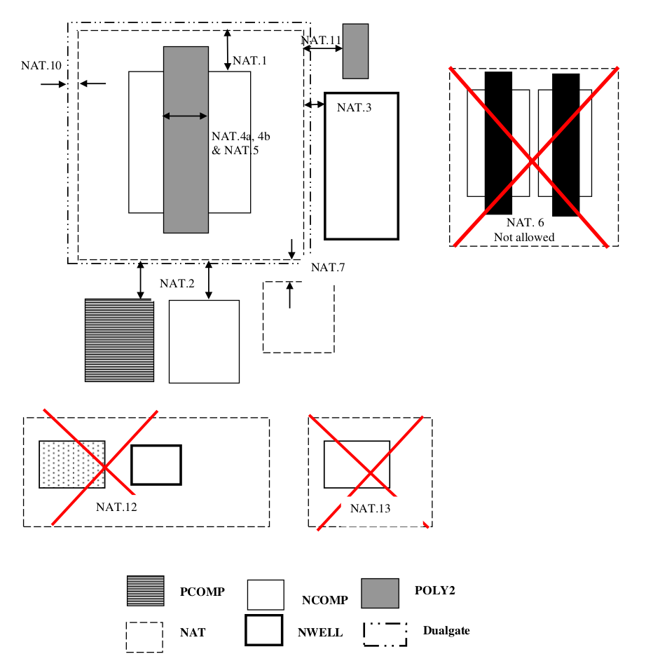
Native Vt NMOS is recognized by NCOMP outside NWELL, interact with Poly2 and NAT.
RULE NO. |
DESCRIPTION |
LAYOUT RULE |
LAYER |
NAT |
|
NAT.1 |
Min. NAT Overlap of COMP of Native Vt NMOS |
2 |
NAT.2 |
Space to unrelated COMP (outside NAT) |
0.3 |
NAT.3 |
Space to NWell edge |
0.5 |
NAT.4 |
Minimum channel length for 3.3V Native Vt NMOS (For smaller L Ioff will be higher than Spec) |
1.8 |
NAT.5 |
Minimum channel length for 6.0V Native Vt NMOS (For smaller L Ioff will be higher than Spec) |
1.8 |
NAT.6 |
Two or more COMPs if connected to different potential are not allowed under same NAT layer |
|
NAT.7 |
Minimum NAT to NAT spacing |
0.74 |
NAT.8 |
Min. Dualgate overlap of NAT (for 5V/6V) native VT NMOS only |
0 |
NAT.9 |
Poly interconnect under “NAT” layer is not allowed min spacing of un-related poly from the NAT layer |
0.3 |
NAT.10 |
Nwell,inside “NAT” layer are not allowed |
|
NAT.11 |
NCOMP not intersecting to Poly2, is not allowed inside “NAT” layer |
|
NAT.12 |
Poly2 not intersecting with COMP is not allowed inside “NAT” (Poly2 resistor is not allowed inside “NAT”) |