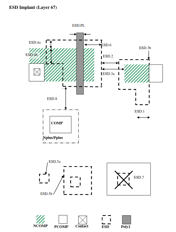
7.11 ESD Implant
This is optional for ESD performance improvement of 5V/6V I/O devices only.
RULE NO. |
DESCRIPTION |
LAYOUT RULE |
Layer |
ESD = ESD Implant |
|
ESD.1 |
Minimum width of an ESD implant area |
0.6 |
ESD.2 |
Minimum space between two ESD implant areas (Merge if the space is less than 0.6um) |
0.6 |
ESD.3a |
Minimum space to NCOMP |
0.6 |
ESD.3b |
Min/max space to a butted PCOMP |
0 |
ESD.4a |
Extension beyond NCOMP |
0.24 |
ESD.4b |
Minimum overlap of an ESD implant edge to a COMP |
0.45 |
ESD.5a |
Minimum ESD area |
0.49 μm2 |
ESD.5b |
Minimum field area enclosed by ESD implant |
0.49 μm2 |
ESD.6 |
Extension perpendicular to Poly2 gate |
0.45 |
ESD.7 |
No ESD implant inside PCOMP |
|
ESD.8 |
Minimum space to Nplus/Pplus |
0.3 |
ESD.PL |
Minimum gate length of 5V/6V gate NMOS |
0.8 |
ESD.9 |
ESD implant layer must be overlapped by Dualgate layer (as ESD implant option is only for 5V/6V devices) |
|
ESD.10 |
LVS_IO shall be drawn covering I/O MOS active area by minimum overlap |
0 |